Hybrid Bonding: Pioneering the Future of Chip Manufacturing
The world of microelectronics is constantly evolving, and at the heart of this transformation is the Hybrid Bonding Technology market. This revolutionary technology is redefining how semiconductor packaging is done, enabling smaller, faster, and more energy-efficient devices. Whether it's powering the next generation of smartphones, AI processors, or 5G networks, hybrid bonding is a critical component in ensuring these devices operate at peak performance.
Unlike traditional bonding methods, hybrid bonding provides a more refined solution for stacking chips at an ultra-fine pitch, dramatically improving the performance and functionality of integrated circuits. This makes it an essential technology for advanced chip architectures, including 3D integrated circuits (3D ICs) and chiplets.
Hybrid Bonding Technology Market Overview
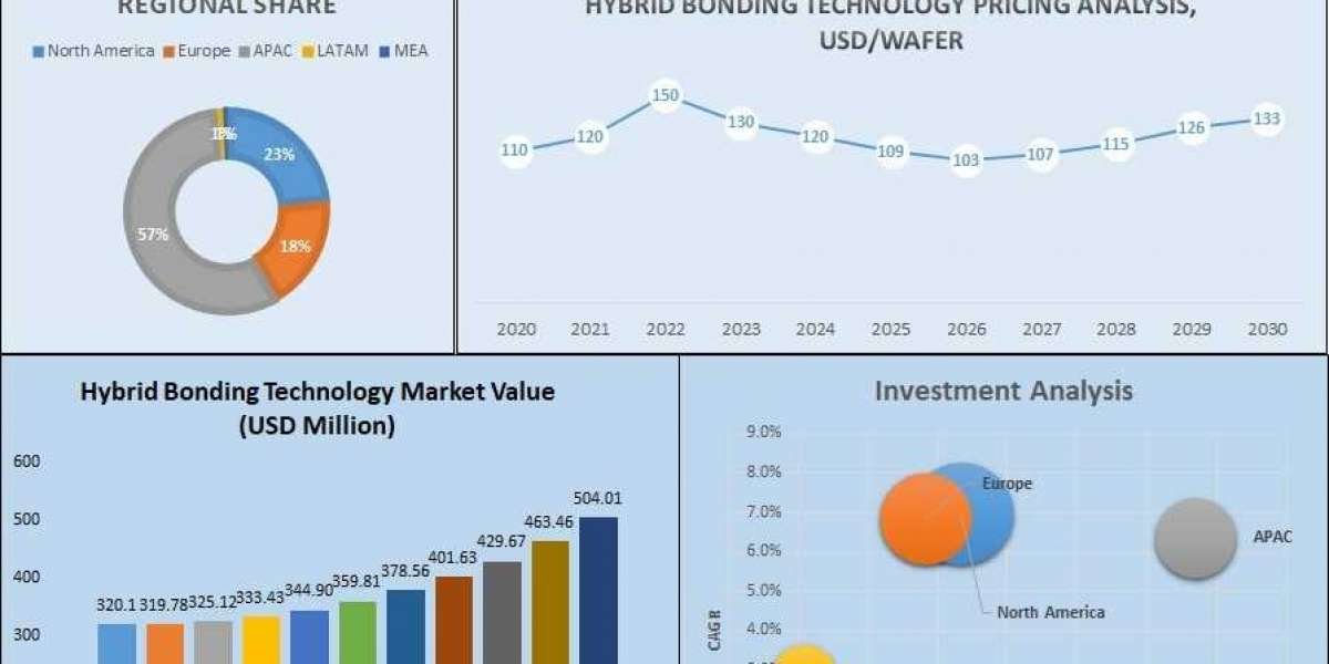
The Hybrid Bonding Technology market was valued at USD 333.43 million in 2023 and is projected to reach USD 504.01 million by 2030, growing at a CAGR of 6.5% from 2024 to 2030. This significant growth signals the increasing reliance on hybrid bonding as a key enabler for next-generation electronics.
The market’s expansion is being driven by the continuous need for faster, smaller, and more efficient devices, particularly in industries like consumer electronics, automotive, and telecommunications. As more companies adopt hybrid bonding for its superior performance benefits, the market is expected to keep growing, with key innovations anticipated in packaging and bonding technologies.
Why Is Hybrid Bonding Gaining Popularity?
The rise of the Hybrid Bonding Technology market is tied to several key factors that are reshaping the semiconductor landscape:
Miniaturization demands: As consumers demand smaller devices with better performance, manufacturers must use technologies like hybrid bonding to maintain the balance between size and speed.
5G and AI growth: The rapid expansion of 5G networks and AI applications requires chips that can handle high speeds, bandwidth, and complex processing. Hybrid bonding allows manufacturers to meet these challenges by providing efficient chip-to-chip communication.
3D IC architecture: Hybrid bonding is an essential component of 3D IC designs, enabling stacking chips vertically to increase performance without expanding the chip's footprint.
A Deep Dive into the Hybrid Bonding Technology Market Size
The Hybrid Bonding Technology Market Size highlights the growing importance of this technology in the semiconductor industry. With a clear path for growth, the market offers immense opportunities for companies to innovate and invest in hybrid bonding solutions. As technology continues to evolve, hybrid bonding is expected to play a pivotal role in enabling smaller, faster, and more powerful devices.
Asia-Pacific remains the dominant region for manufacturing, while the U.S. and Europe focus on driving innovation and research in hybrid bonding materials and processes. The market is also seeing increased collaboration between foundries, equipment manufacturers, and RD centers, further accelerating the adoption of hybrid bonding.
Key Takeaways from the Latest Hybrid Bonding Technology Report
The most recent Hybrid Bonding Technology report sheds light on the future direction of the market, focusing on several key trends:
The increasing popularity of die-to-wafer and wafer-to-wafer bonding methods, which are becoming the go-to solutions for advanced packaging.
The industry's focus on improving manufacturing yield and reducing defects, ensuring that hybrid bonding processes are scalable for mass production.
A growing emphasis on partnerships and collaborations, especially between fabless companies and foundries, to speed up the integration of hybrid bonding in next-gen devices.
These insights underscore hybrid bonding’s pivotal role in pushing the boundaries of what’s possible in semiconductor technology.
Conclusion: A Future Built on Hybrid Bonding
As the semiconductor industry advances, the Hybrid Bonding Technology market is set to become a cornerstone of innovation. Its ability to enable more efficient, faster, and smaller chips makes it a vital tool in the development of future technologies, from AI to 5G and beyond.
With an expanding market size and constant innovation, hybrid bonding is poised to play an increasingly critical role in shaping the future of semiconductor manufacturing.
Contact Information:
Company Name: Mark Spark Solutions
Contact Person: Sushil W
Email: sales@marksparksolutions.com
Phone: +1-585-374-1088
Website: https://marksparksolutions.com